V1.0
Fraser innovation inc
FII-BD9361 Hardware Reference Guide
Version Control
| Version | Date | Description |
| V1.0 | 12/03/2019 | Initial Release |
Copyright Notice:
© 2019 Fraser Innovation Inc ALL RIGHTS RESERVED
Without written permission of Fraser Innovation Inc, no unit or individual may extract or modify part of or all the contents of this manual. Offenders will be held liable for their legal responsibility.
Thank you for purchasing the FPGA development board. Please read the manual carefully before using the product and make sure that you know how to use the product correctly. Improper operation may damage the development board. This manual is constantly updated, and it is recommended that you download the latest version when using.
Official Shopping Website:
Fraser Innovation Inc develops BD9361 of perfectly compatible with AD-FMCOMMS3-EBZ – Code compatible, development tool compatible, performance compatible, smaller size and more space saving – The FII-BD9361 board covers all features and benefits of AD9361. The AD9361 is a high performance, highly integrated radio frequency (RF) Agile Transceiver™ designed for use in 3G and 4G base station applications. Its programmability and wideband capability make it ideal for a broad range of transceiver applications.
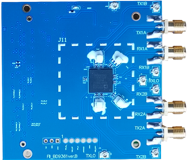
BD9361 Full View Picture 1
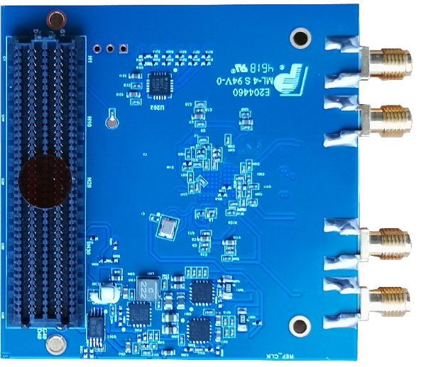
BD9361 Full View Picture 2
Contents
3. Block Diagram and Interface 8
Introduction
The FII-BD9361 is a high-speed analog module designed to showcase the AD9361, a high performance, highly integrated RF transceiver intended for use in RF applications, such as 3G and 4G base station and test equipment applications, and SDR (software defined radios). Its program-ability and wide-band capability make it ideal for a broad range of transceiver applications. The device combines an RF front end with a flexible mixed-signal base-band section and integrated frequency synthesizers, simplifying design-in by providing a configurable digital interface to a processor or FPGA.
The AD9361 chip operates in the 70 MHz to 6 GHz range, covering most licensed and unlicensed bands. The chip supports channel bandwidths from less than 200 kHz to 56 MHz by changing sample rate, digital filters, and decimation, which are all programmable within the AD9361 itself.
Basic Features
- Software tunable across wide frequency range: TX :47 MHz to 6 GHz RX:70 MHz to 6 GHz
- Software tunable bandwidth: 200 kHz to 56 MHz
- Software tunable TX Power and RX Dynamic Range: TX>80dB RX>70dB
- Powered up from single standard FMC connector
- Supports MIMO radio,2 ways TX and 2 ways RX
- Supports FII-7030 and other standard FMC Connector Platform software radio application
- Size dimensions:690X690cm (PCB only),690X790mm (with SMA Connectors)
Block Diagram and Interface
System Block Diagram
| Interface Type | Definition | Description |
| SMA-F | TX1A, TX2A | 2 x RF transmission channel (same frequency) |
| SMA-F | RX1A, RX2A | 2 x RF receiving channel (same frequency) |
| UMC-F | TX1B, TX2B | 2 x RF transmission channel (reference to channel A) |
| UMC-F | RX1B, RX2B | 2 x RF transmission channel (reference to channel B) |
| UMC-F | TXLO | External transmission reference oscillator |
| UMC-F | RXLO | External receiving reference oscillator |
| UMC-F | REF | External reference clock |
| LPC FMC | FMC | Refer the schematics for universal RF transmission interface, compatible with similar products in most markets |
Peripheral interface table
FMC-LPC Definition
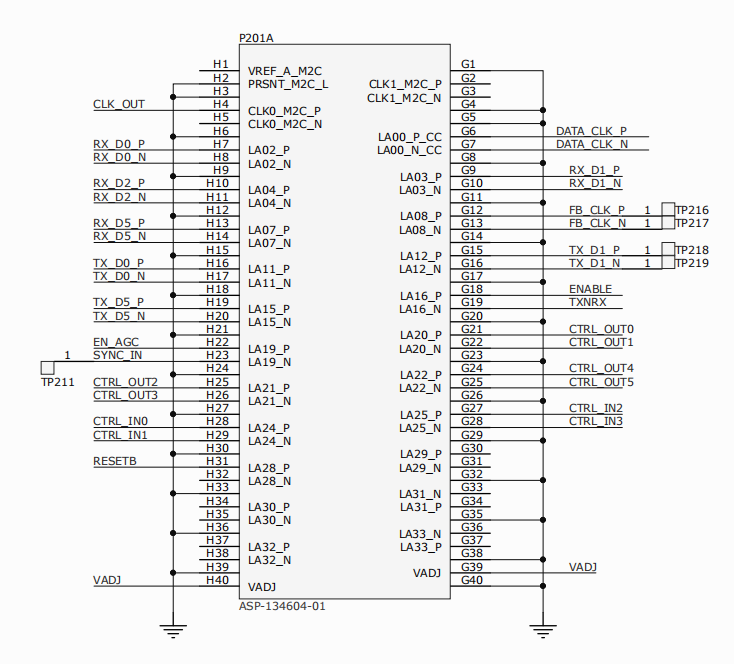
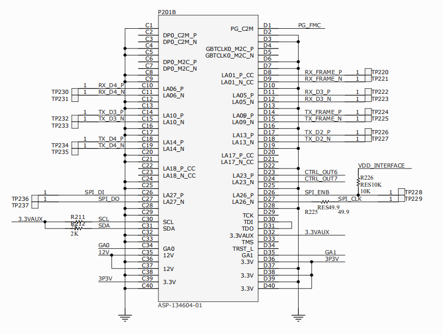
FMC-LPC Definition (compatible with AD-FMCOMMS3)
Compatible Board
AD-FMCOMMS3-EBZ (Same as FII-BD9361)
(https://www.analog.com/en/design-center/evaluation-hardware-and-software/evaluation-boards-kits/eval-ad-fmcomms3-ebz.html#eb-overview)
References
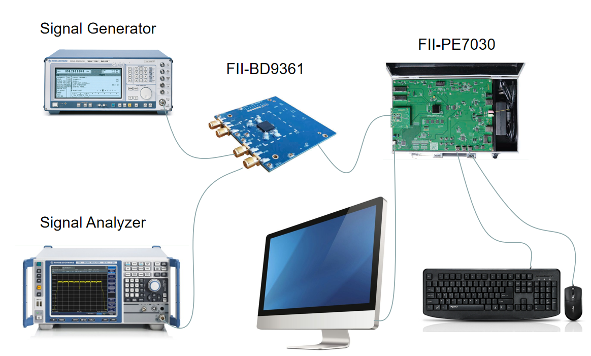
Test case setup
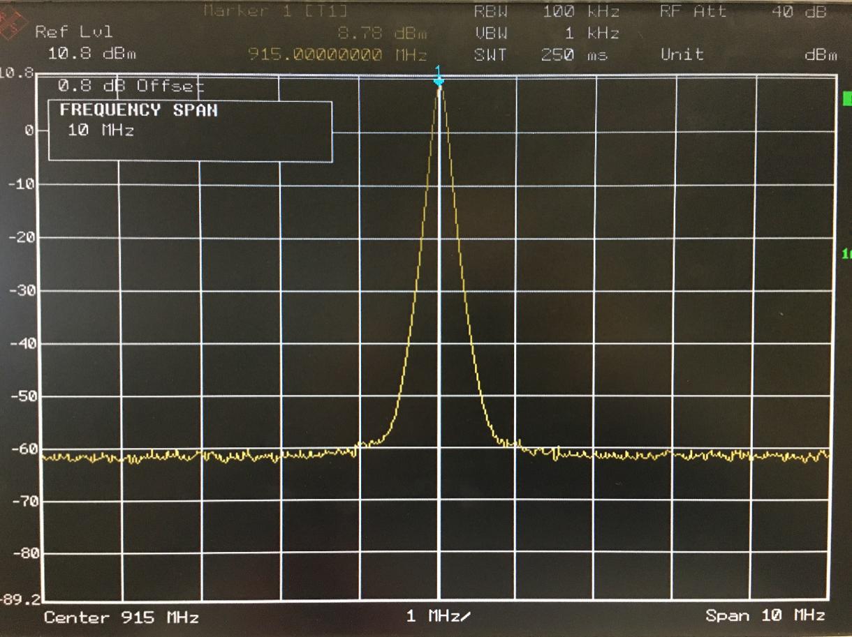
Output power and flatness test under 0.8 dB offset 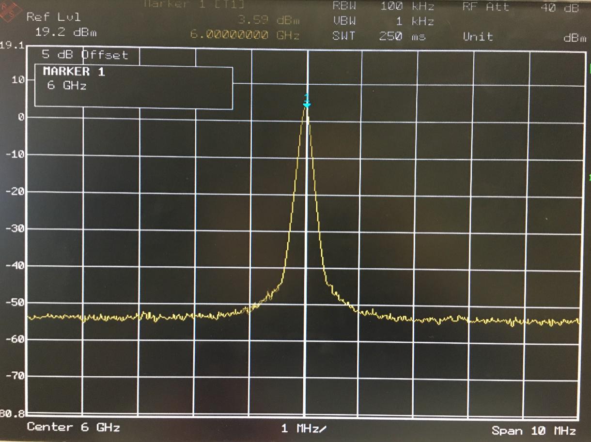
Output power and flatness test under 5 dB offset
The above picture is a screenshot of some tests. The frequency range covers 70MHz to 6GHz, and the output power from 150MHz to 6GHz is 3-8dBm. The high-performance RF Balun design guarantees high bandwidth and high flatness.
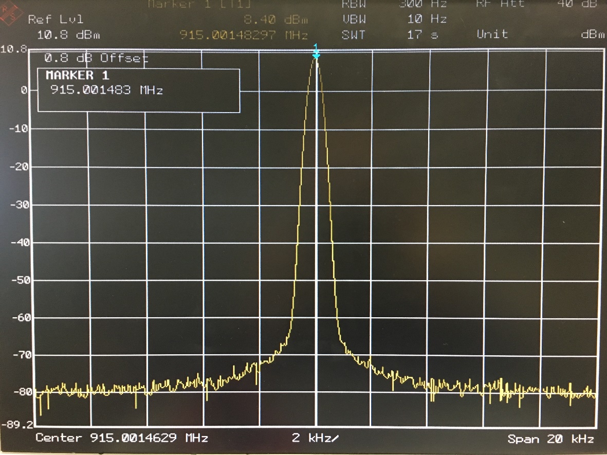
Phase noise test under 0.8 dB offset
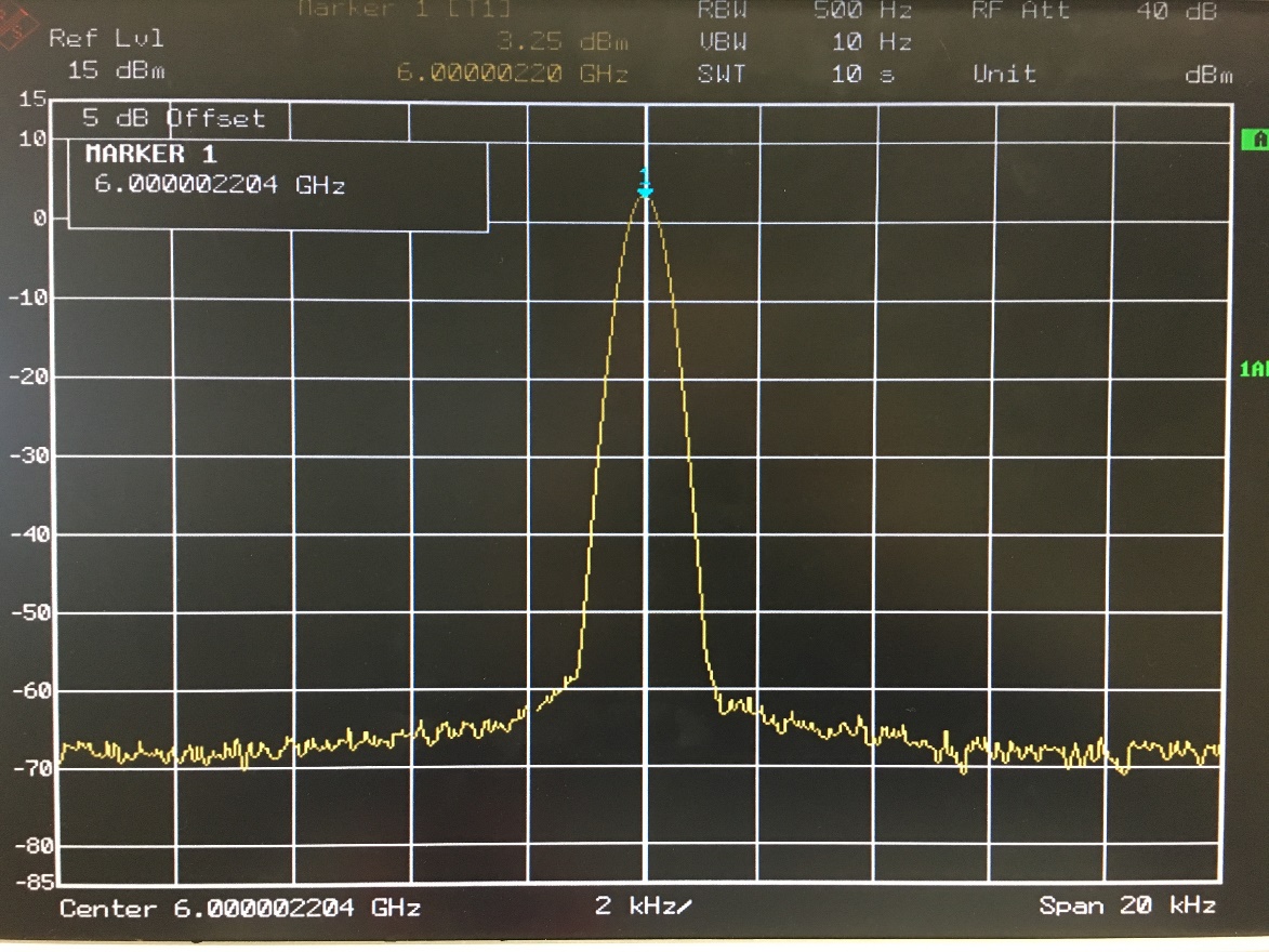
Phase noise test under 5 dB offset
The picture above is a screenshot of some tests. The frequency range covers 70MHz to 6GHz. Typical 6GHz phase noise is 90dBc / 1KHz, 100dBc / 10KHz. The perfect phase noise guarantees high-quality communication test requirements.
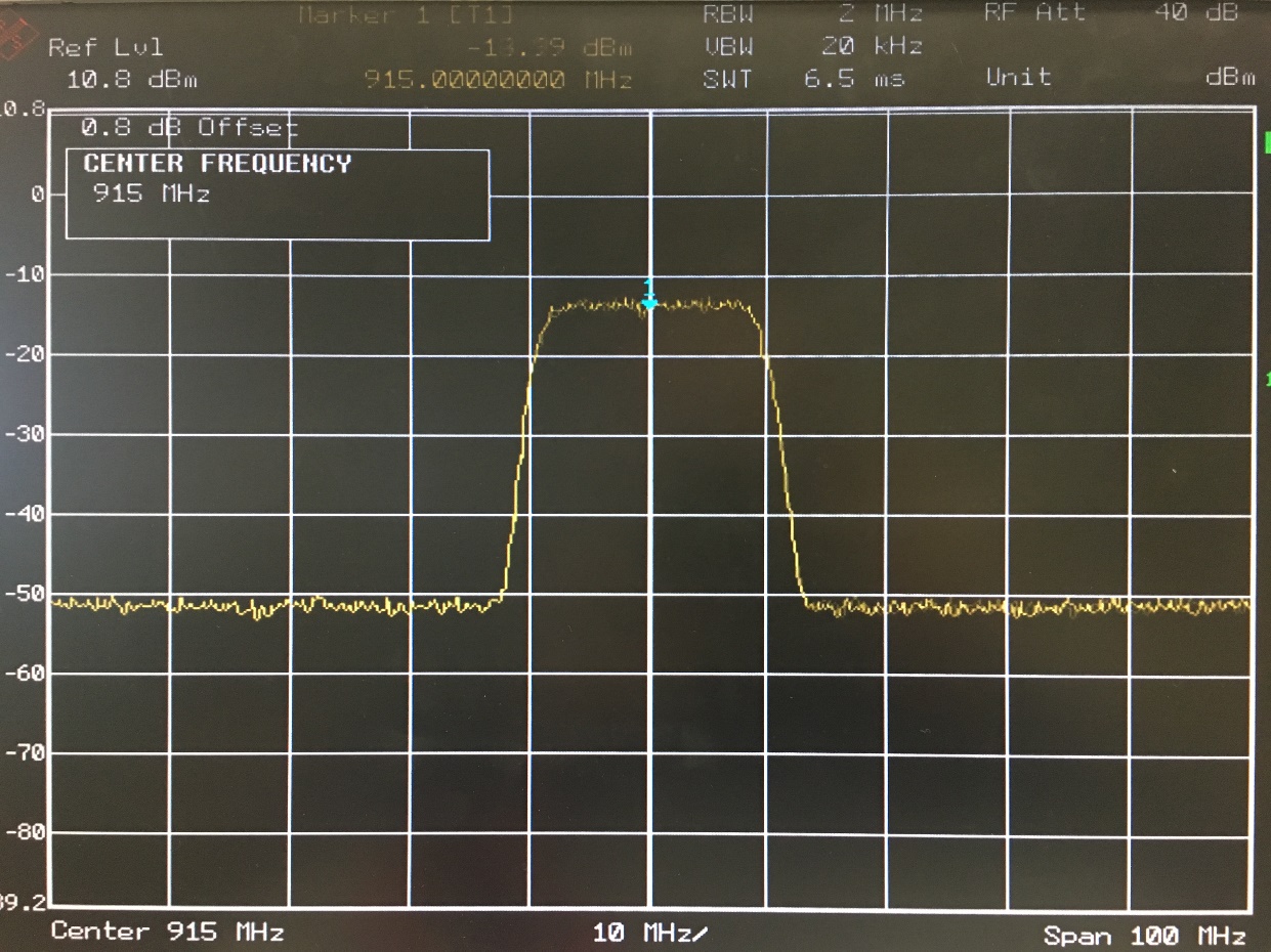
IQ modulation function test
The figure above shows the spectrum output of the IQ signal QPSK modulated signal at the frequency of 915MHz and 20MHz bandwidth.
